PHMe22 | 7th European Conference of the Prognostics and Health Management Society 2022
Bitron Electronics will take centre stage of PHMe22, the 7th European Conference of the Prognostics and Health Management Society 2022, which will took place in Italy at Turin, from 6 to 8 July. In this edition of the PHME Data Challenge, to which more than 27 groups from 9 nations have already signed up, participants are challenged to demonstrate the application of state-of-the-art algorithms and models to solve a classification problem for a Bitron Electronics real production line.
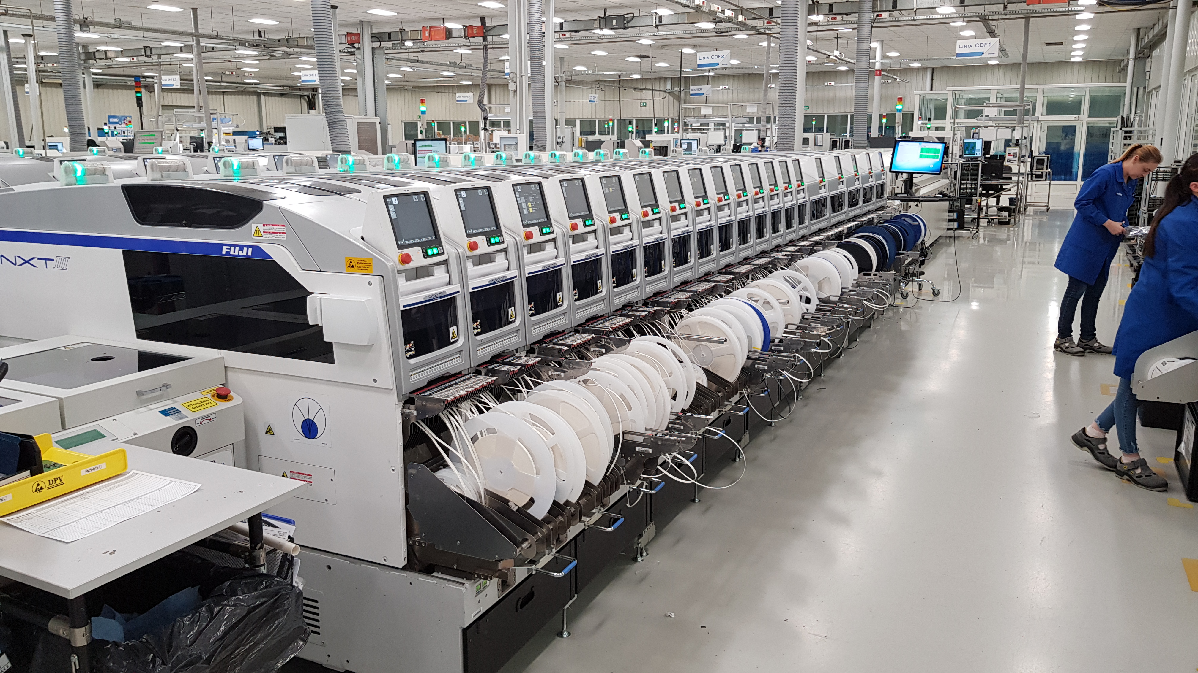
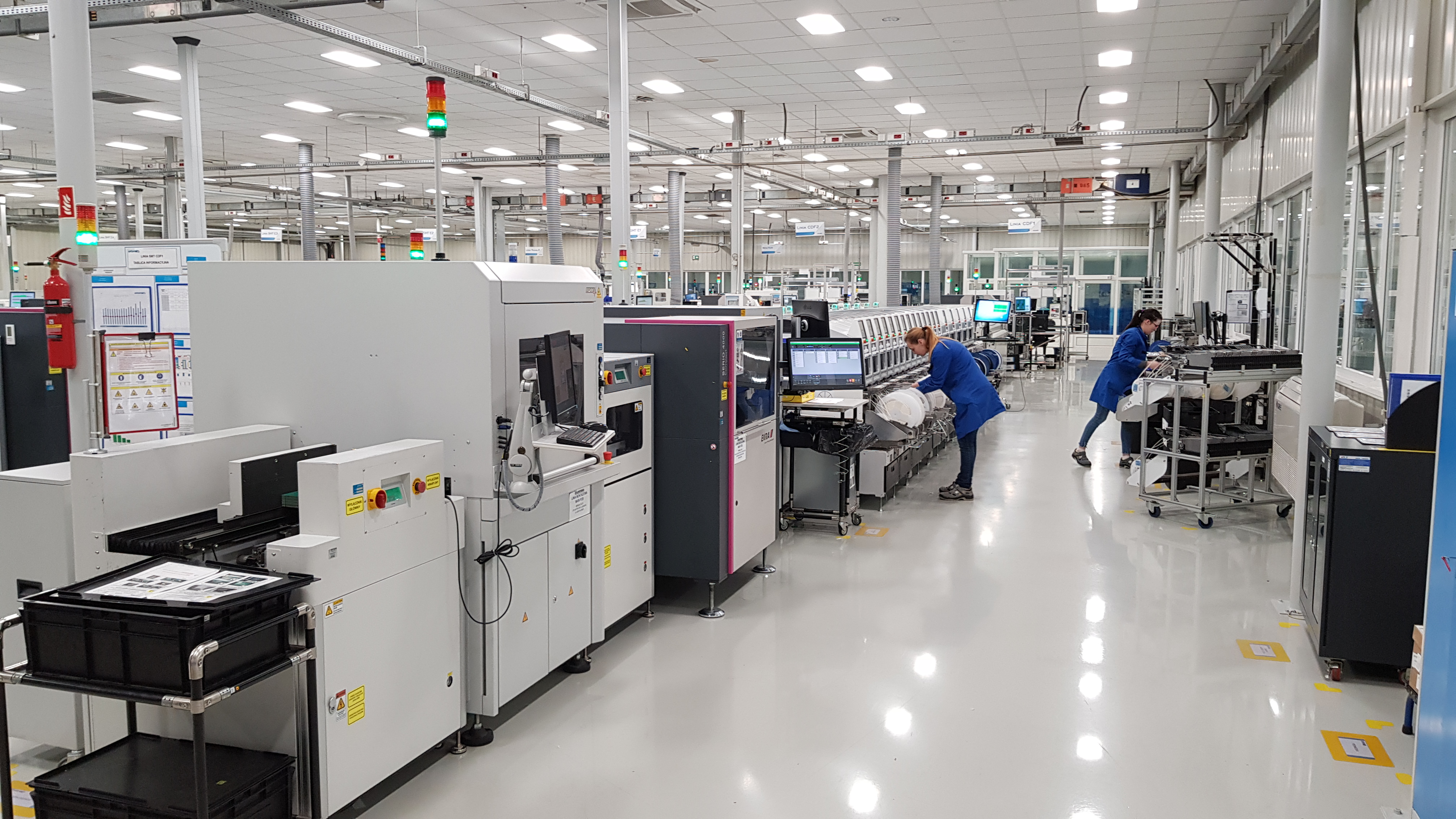
The competition has exclusive access to an extensive dataset of a real industrial production line equipped with automated, integrated and fully connected machines and the final goal for the teams will be to design an algorithm to predict the defect labels for the components. In detail, during the production line, the PCB goes through the following steps:
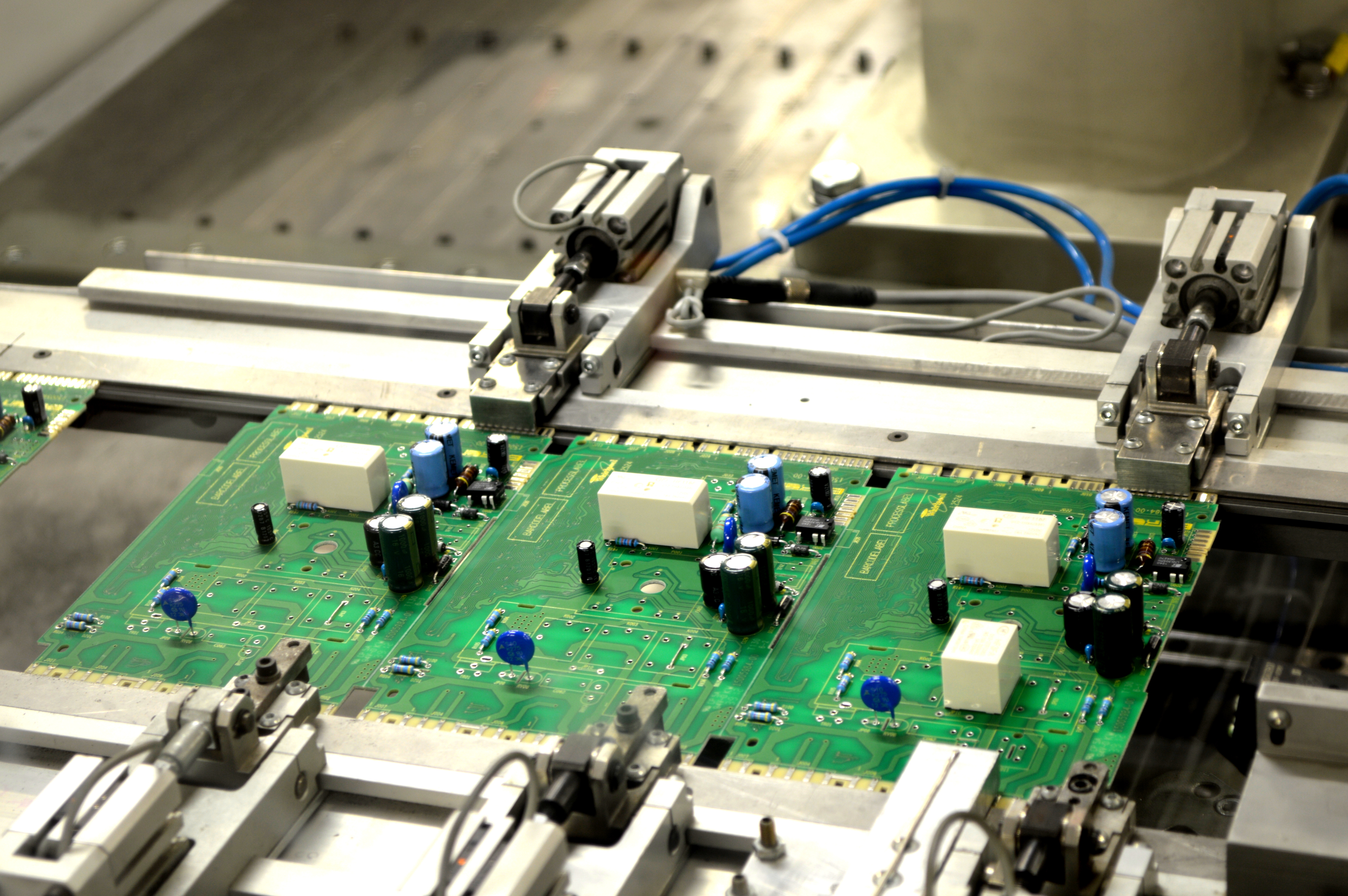
- The printing machine: initially, by using a laser prints a serial number on the PCB and then places the solder paste.
- Solder paste inspection (SPI): checks the solder paste placed by the printing machine placed to identify possible problems, e.g. too much/missing paste, short circuit, etc. It stores rich metadata.
- Surface mount device (SMD) placement: places the electronic components on the PCB.
- Reflow oven: reflows the solder paste in a molten state to create permanent solder joints.
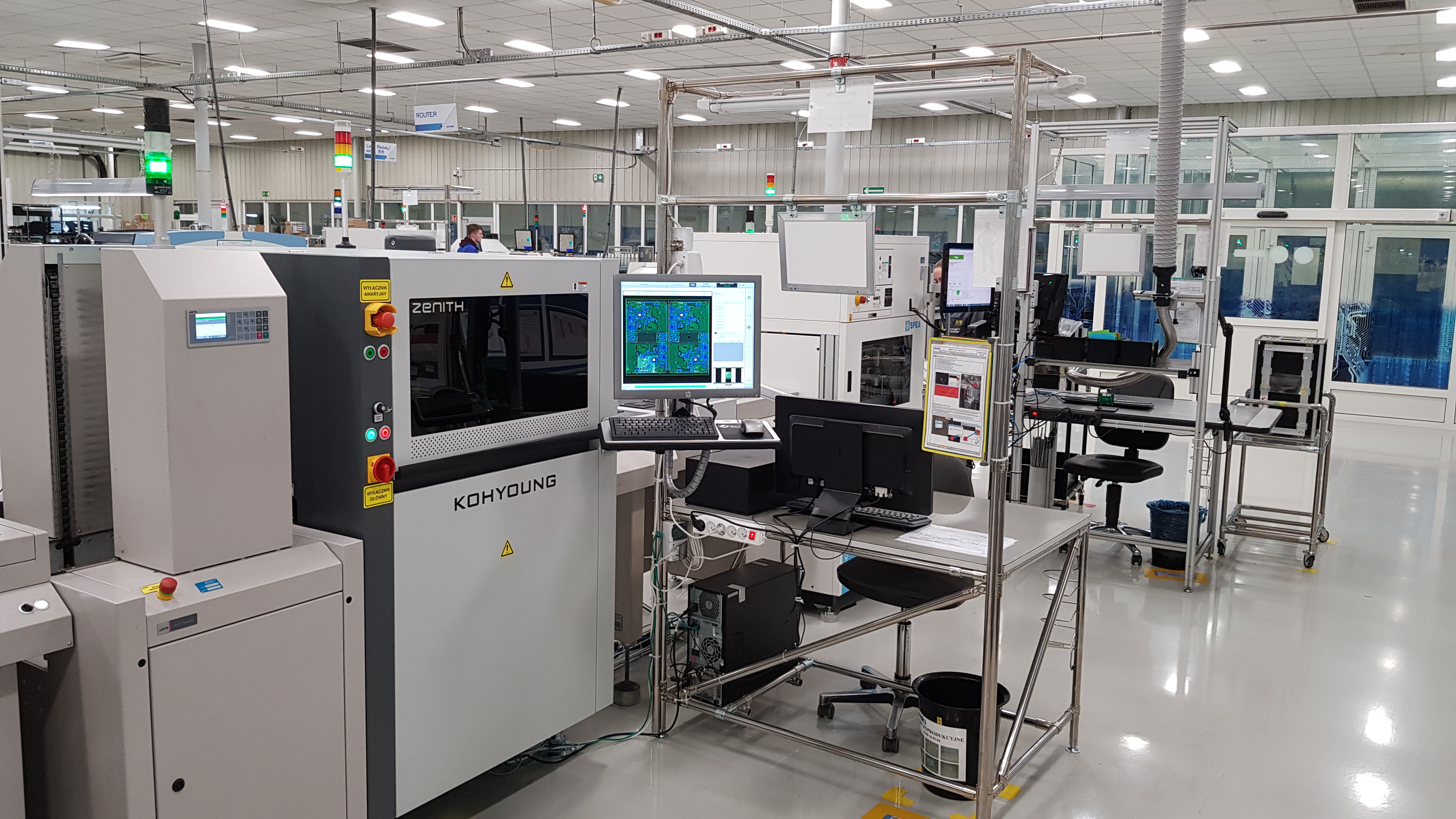
- Automatic Optical Inspection (AOI): automatically inspects the PCB to detect defects in the previous steps, e.g., missing components, fillet size or shape of fillets, or misalignment of components, etc.
During the challenge, the teams gain access to the data from the Solder Paste Inspection (SPI) and the Automated Optical Inspection (AOI) machines. The datasets provided by these machines will be used for the prediction of the quality damages of the final products. The data were collected during the real manufacturing of PCBs under normal conditions. In this scenario, the SPI data, reports, for each PCB, characteristics such as:
- Identifiers: PanelID, FigureID, ComponentID, PinNumber
- Soldering paste characteristics: Volume, Area, Height, Shape, Results
While the AOI data describe, for PCB each defect highlighted by the machine, characteristics such as:
- Identifier: PanelID, FigureID, ComponentID
- Defect labels: label according to the AOI machine, a label applied by the operator after visual inspection, a label applied by a second operator based on the possibility of repair.
- The goal is to design an algorithm to predict the defect labels for the components. Specifically, the goal is to develop a hierarchical classification predicting: (i) whether the AOI classifies the component as defective; (ii) in the case of a defect, the label applied by the operator; (iii) in the case of confirmation of the defect by the operator, the repair label.
The ultimate goal of this classification system is to improve the efficiency of the PCB manufacturing process, facilitate the operator’s work and minimize the cases of manual intervention. A performing classification model can help the operator identify the components to be reworked after the SPI step, reducing the number of images she has to process.
The dataset used for training and validation of the model will be made available immediately after the start of the competition. The use of data-driven and physics-based modelling approaches is encouraged. To standardize the final performance evaluation, a standard Python script will be provided during the competition period. The teams are also encouraged to use the online Data Science environment offered by Politecnico di Torino to work on their solution. This also allows the teams to be part of the leader board and evaluate their progress day by day.
Winning teams will be asked to write a full manuscript that will be published in the PHM conference proceedings, and a representative will be expected to give an oral presentation at the event. The award will be presented at the conference social event.
Find out more on https://phm-europe.org/data-challenge